
What inspired you to study these tiny materials, and why are they important for future technologies?
My interest in these materials comes from a broader curiosity about how materials behave at extremely small scales. When materials are reduced to the nanoscale, their properties can change in remarkable ways compared to their bulk counterparts. These differences often create opportunities for new scientific discoveries and technological innovations. Transition metal chalcogenides are particularly exciting because they combine a unique layered structure with tunable electrical, optical, and chemical properties. Researchers around the world are studying them to develop improved energy storage systems, efficient catalysts for clean energy production, and advanced electronic devices. By understanding how their structure influences their properties, we can design materials that perform better and are more sustainable for future technologies.
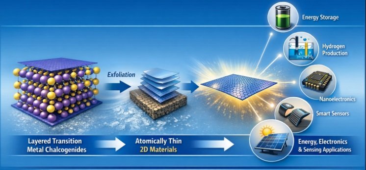
In simple terms, what are transition metal chalcogenides, and what makes them special compared to other materials?
Transition metal chalcogenides are compounds formed by combining a transition metal element, such as molybdenum, tungsten, titanium, or vanadium, with a chalcogen element like sulfur, selenium, or tellurium. One of the most distinctive features of these materials is their layered crystal structure. Each layer consists of a transition metal atom sandwiched between two chalcogen atoms, forming a stable sheet only a few atoms thick. These sheets stack together to form the bulk material, but the forces holding the layers together are relatively weak. Because of this structure, scientists can isolate individual layers, creating 2D materials like graphene. These ultrathin layers exhibit fascinating properties such as tunable semiconducting behavior, strong catalytic activity, and unique optical responses. These characteristics make transition metal chalcogenides highly attractive for a wide range of scientific and technological applications.
Your research focuses on very thin materials. Why does making materials thinner change their properties?
When materials become extremely thin, sometimes only one or a few atomic layers thick, their physical behavior changes significantly. At this scale, the movement of electrons and the interactions between atoms are strongly influenced by quantum mechanical effects. Another important factor is surface area. In very thin materials, a larger proportion of atoms is located at or near the surface This increases the number of active sites available for chemical reactions, which is especially useful for catalytic applications. Also, the electronic structure of the material can change as the number of layers decreases. For example, some transition metal dichalcogenides shift from indirect to direct bandgap semiconductors when reduced to a single layer, which greatly enhances their optical and electronic performance. These changes make ultrathin materials extremely valuable for nanotechnology.
How can these tiny materials help improve energy technologies like batteries or hydrogen production?
Transition metal chalcogenides are being widely explored for their potential in energy-related applications. In battery technologies, their layered structure allows ions such as lithium, sodium, or zinc to move efficiently between layers. This property can improve energy storage capacity and enable faster charging and discharging processes. Researchers are also investigating their stability and conductivity to design better electrode materials. In hydrogen production, these materials can function as catalysts for the hydrogen evolution reaction during water splitting. Catalysts help accelerate chemical reactions, and certain transition metal chalcogenides have demonstrated strong catalytic activity while being significantly less expensive than traditional noble-metal catalysts like platinum. This makes them promising materials for large-scale renewable hydrogen generation.
Can these materials help make electronic devices smaller, faster, or more efficient? If yes, how?
Yes, these materials have strong potential to transform modern electronics. Because transition metal chalcogenides can be fabricated as atomically thin layers, they allow engineers to design electronic components at extremely small dimensions. Their semiconducting properties make them particularly attractive for building next-generation transistors, which are the fundamental components of electronic circuits. In addition, their flexibility allows them to be integrated into bendable or wearable electronic devices. Also, their optical and electronic properties enable applications in photodetectors, light-emitting devices, and advanced sensors. As research is progressing, these materials could help create electronic systems that are both more powerful and more energy efficient.
What are some real-world applications where we might see these materials used in the future?
In the future, transition metal chalcogenides could play an important role in several advanced technologies. They may be used in high-performance batteries and supercapacitors that store energy more efficiently. They could also serve as catalysts for hydrogen production and other clean energy processes. In electronics, they may enable flexible devices, transparent circuits, and highly sensitive sensors. In addition, their optical properties make them promising materials for photodetectors and next-generation optoelectronic devices. As research and engineering efforts continue, these materials may gradually move from laboratory studies to commercial technologies.
What are the biggest challenges scientists face when developing and using these advanced materials?
Despite their exciting potential, several scientific and engineering challenges remain. One major challenge is producing these materials in large quantities with consistent quality and controlled thickness. Many current synthesis methods are suitable for laboratory research but need further development for industrial-scale manufacturing. Another challenge is controlling structural defects and variations in composition, which can strongly influence the performance of the material. Researchers across the globe are also working on improving the stability of these materials and integrating them effectively into real devices. Addressing these challenges requires collaboration between chemists, materials scientists, physicists, and engineers.
What exciting discoveries or technologies do you expect to see in this field over the next 10 years?
Over the next decade, the field of 2D materials is likely to grow rapidly. We can expect significant progress in both fundamental understanding and practical applications. Researchers may develop highly efficient catalysts for green hydrogen production, advanced battery materials with higher energy density, and flexible electronics integrated into everyday devices such as wearable health monitors. We may also see breakthroughs in nanoscale sensors and optoelectronic technologies. As our ability to control materials at the atomic level improves, these tiny materials could become key components in future energy systems and electronic technologies.


