
The increasing global demand for energy continues to depend heavily on conventional resources such as coal, oil, natural gas, and nuclear power. Rapid industrialisation, electrification of transportation, rising cooling demands, and the expansion of data centres have further accelerated energy consumption. However, the excessive use of fossil fuels has significantly increased carbon dioxide emissions, leading to serious environmental and climate-related concerns. To reduce greenhouse gas emissions and achieve sustainable development, renewable energy technologies are being actively explored. Among them, hydrogen energy has emerged as one of the most promising clean energy solutions. Hydrogen is considered an environmentally friendly fuel because it possesses a very high gravimetric energy density of approximately 120 MJ kg⁻¹ and produces only water vapour during combustion. Its energy density is nearly three times higher than gasoline, making it highly attractive for fuel-cell vehicles and future clean energy technologies. Hydrogen can be produced by water splitting reactions [Nature 238, 37–38 (1972)]. The water splitting process requires a minimum thermodynamic energy of 237 kJ mol⁻¹ or 1.23 V. In 1972, Akira Fujishima and Kenichi Honda first demonstrated photoelectrochemical water splitting using an n-type titanium dioxide (TiO₂) semiconductor electrode under ultraviolet irradiation, commonly known as the Honda–Fujishima effect. This discovery established semiconductor materials as important candidates for solar-driven hydrogen production. However, TiO2 possesses a wide band gap of approximately 3.2 eV and absorbs only ultraviolet light, which represents nearly 5% of the solar spectrum. In addition, bulk semiconductor materials often suffer from rapid recombination of photogenerated electrons and holes, limiting their photocatalytic efficiency. Their relatively low surface-to-volume ratio also reduces the number of active catalytic sites available for water splitting reactions. Semiconductor nanomaterials overcome many of these limitations because of their nanoscale dimensions and large surface-to-volume ratio. The increased surface area enhances interaction between water molecules and catalytically active sites, thereby improving hydrogen generation efficiency. Moreover, reducing the size of semiconductor nanomaterials produces quantum confinement effects that modify their electronic structures and charge carrier dynamics. These effects help suppress electron–hole recombination and improve the reduction and oxidation potentials required for water splitting. Consequently, semiconductor nanostructures have become highly promising materials for clean and sustainable hydrogen production.
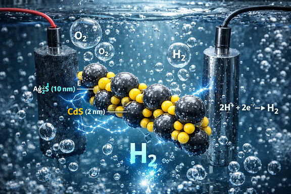
Band gap engineering through semiconductor heterostructure formation further improves light absorption and charge separation efficiency. Combining a wide band gap semiconductor with a narrow band gap material extends optical absorption from the ultraviolet region into the visible and near-infrared regions of the solar spectrum. More importantly, the heterostructure interface controls the movement and separation of photogenerated electrons and holes under light illumination. Cadmium sulfide (CdS) is one of the most widely investigated semiconductor materials for hydrogen evolution because of its suitable band gap of approximately 2.42 eV, which allows strong visible-light absorption. Highly quantum-confined CdS quantum dots with particle sizes below 4 nm exhibit improved charge separation and reduced recombination compared with bulk semiconductor systems. As a result, CdS nanomaterials demonstrate higher photocatalytic hydrogen generation efficiency than TiO2. However, CdS-based photocatalytic systems often suffer from photocorrosion and photobleaching during long-term operation. To overcome these limitations, CdS has been combined with silver sulfide (Ag2S), a narrow band gap semiconductor with a band gap of approximately 0.9–1.0 eV. The incorporation of Ag2S broadens the optical absorption range from ultraviolet to infrared wavelengths and improves charge transport properties. In addition, the CdS–Ag₂S interface promotes efficient separation and transfer of photogenerated charge carriers, thereby enhancing photoelectrochemical hydrogen production. Conventional CdS–Ag₂S heterostructures prepared in patchy, core–shell, type-I, or type-II configurations often exhibit poor surface charge passivation and weak electronic coupling. In type-I heterostructures, the narrow- band gap semiconductor is generally located at the core while the wider- band gap material forms the shell, resulting in charge confinement within the nanostructure. In contrast, type-II heterostructures spatially separate electrons and holes between two semiconductor domains, improving charge separation and reducing recombination losses. A more advanced strategy involves the synthesis of semiconductor superlattice heterostructures. In these systems, periodically arranged heterostructures generate electronically coupled miniband states that facilitate rapid charge transport and enhanced light–matter interaction. Superlattice structures possess strongly quantum-confined electronic states and improved interparticle coupling, making them highly effective for photocatalytic and electrochemical applications. Such nanostructures can be fabricated using methods such as electron-beam epitaxy, vapour–liquid–solid growth, electron-beam lithography, and cation or anion exchange reactions. The first colloidal superlattice nanostructures were reported by C. B. Murray and co-workers in 1995, demonstrating their importance for optoelectronic applications [Science 270 (1995); 1335-1338]. Later, Alivisatos et. al. reported spontaneous CdS–Ag2S nanorod superlattice formation by cation exchange reactions in colloidal systems [Science 317 (2007), 355]. We successfully developed ordered CdS–Ag2S nanorod superlattices by a dual molecular source synthesis approach. The diffusion behaviour and miniband formation within the CdS–Ag2S heterostructures were controlled using thiocarboxylate molecular precursors, namely (PPh3)2Ag(SCOPh) and Cd(SCOPh)2, together with dodecane thiol (DDT) and octadecyl amine (ODA) surface ligands. The presence of triphenylphosphine and the associative interaction of DDT ligands promoted the formation of highly ordered one-dimensional superlattice architectures. X-ray photoelectron spectroscopy studies of the thiol-capped CdS–Ag2S nanorod superlattice revealed strong polarisation of the CdMMN valence band and electron transfer from Cd 3d and Ag 3d orbitals toward the S 2p states. These observations confirmed strong electronic coupling and efficient charge redistribution within the superlattice structure. In contrast, ODA-capped CdS–Ag₂S quantum dot superlattices exhibited disordered atomic packing with weaker electronic interaction, leading to electron transfer mainly from Cd 3d and S 2p orbitals toward Ag 3d states. Furthermore, conventional CdS–Ag₂S heterostructures showed negligible shifts in Cd 3d, Ag 3d, and S 2p spin-orbit energies, indicating poor surface charge passivation. Photophysical studies further demonstrated the advantages of the superlattice architecture. The DDT-capped one-dimensional CdS–Ag2S nanorod superlattice displayed a dominant fast charge-carrier recombination component with a lifetime of 0.95 ± 0.007 ns associated with band-edge emission and minimal non-radiative surface trap states. This behaviour indicates efficient charge transport and reduced trapping losses. In contrast, ODA-capped zero-dimensional CdS–Ag2S quantum dot superlattices exhibited dual-band emission caused by disordered atomic packing and increased surface trap formation. These structures showed short-lived band-edge recombination with a lifetime of 0.90 ± 0.008 ns together with long-lived surface-trap emissions centred at 670 nm, with an average carrier lifetime of 78.8 ± 1.00 μs. Overall, our findings demonstrate that ordered CdS–Ag2S superlattice nanostructures significantly improve light absorption, charge separation, and electronic transport compared with conventional heterostructures.
This study does not include photoelectrochemical water-splitting studies on indium tin oxide (ITO) or fluorine-doped tin oxide (FTO)-based superlattice devices. In future, optimising the ultrafast charge-carrier dynamics and interfacial charge transfer of nanorod superlattices on n-type ITO/FTO electrodes remains a major challenge for next-generation clean hydrogen and renewable energy applications.


