
Over the past few decades, scientists have extensively explored ways to manipulate the optical properties of semiconductor nanocrystals, which are tiny crystalline materials whose behaviour is governed by quantum mechanics because of their nanoscale dimensions. Doping in nanocrystals is an intriguing and powerful strategy to further tailor their light absorption and emission behaviour. In this process, impurity atoms are intentionally introduced into the nanocrystal lattice in a controlled manner to modify its electronic structure. Through this approach, both homovalent and heterovalent p-type dopants have demonstrated a wide range of useful functionalities and promising applications in tunable solid-state lighting, fluorescence upconversion, biomedical imaging, photoinduced magnetism, luminescent solar concentrators, and many other optoelectronic technologies.
“For many years, scientists believed that certain impurity atoms could not emit light. In our study, we show that these ‘silent’ atoms can, in fact, produce a distinct and stable glow.”
Despite these advances, one fundamental question remained unresolved: can n-type heterovalent dopants actively participate in light emission in semiconductor nanocrystals? For many years, the answer appeared to be no.
In semiconductor physics, doping is a powerful way to engineer new electronic states within the band gap. In II-VI semiconductors such as CdSe, p-type dopants like copper or silver are known to create localized acceptor states near the valence band. These states can trap photoexcited holes, leading to the formation of acceptor-bound excitons, quasiparticles that radiatively recombine to produce broad, tunable light emission. This phenomenon has been extensively studied and underpins many important optoelectronic applications. n-type dopants (e.g. indium), however, have traditionally behaved very differently. Indium, as a dopant, generally donates electrons directly to the conduction band, thereby enhancing electrical conductivity without substantially affecting radiative recombination processes. Thus, donor-bound excitons, the n-type analogue of acceptor-bound excitons, remained elusive in semiconductor nanocrystals for a long time.
This raised a deeper scientific curiosity: are donor states truly optically inactive, or have they simply remained hidden because of experimental limitations?
To address this question, we turned to a unique class of host nanostructures: two-dimensional CdSe nanoplatelets. Unlike conventional quantum dots, which often exhibit size and shape heterogeneity that lead to broad emission spectra, whereas nanoplatelets possess atomically precise thickness and exceptional structural uniformity. As a result, they exhibit extremely narrow emission linewidths, making them an ideal platform for resolving subtle spectral features that would otherwise remain obscured. Using a colloidal growth-doping strategy, indium atoms were introduced into the CdSe lattice during nanoplatelet formation. Precise control over precursor chemistry proved crucial, as only specific reaction conditions allowed indium ions to substitute cadmium sites without disrupting the crystal structure. Under these optimized conditions, the nanoplatelets retained their two-dimensional morphology while incorporating indium atoms in a controlled manner.
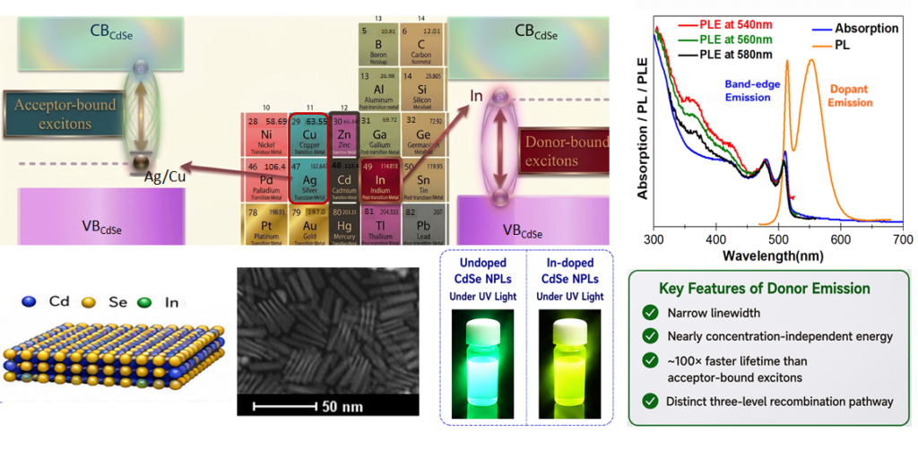
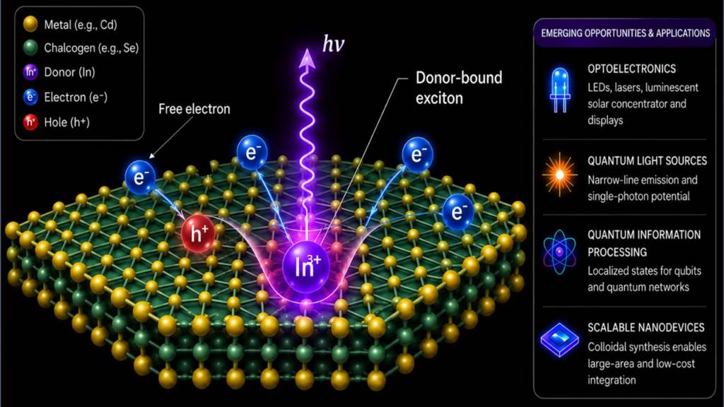
Following indium doping, the absorption spectra remained largely unchanged, and the characteristic band-edge emission of CdSe nanoplatelets was preserved. However, a new and well-separated emission peak emerged alongside the original band-edge signal. The photoluminescence excitation (PLE) spectrum of the new emission peak closely matches the absorption profile of CdSe nanoplatelets, with no evidence of thicker nanoplatelets or quantum dots subpopulations. This confirmed that the new feature originated from the indium-doped nanoplatelets themselves rather than from secondary nanostructures. Detailed spectroscopic analysis confirmed that the new feature originated from a donor-bound exciton, formed when a localized electron associated with the indium donor state recombined with a photo-generated hole. Unlike acceptor-bound excitons, which typically exhibit broad and strongly Stokes-shifted emission, the donor-bound exciton displayed a remarkably narrow emission linewidth and only a small Stokes shift. Even more intriguingly, its emission energy remained nearly unchanged across different dopant concentrations. In p-type-doped systems, increasing the dopant concentration alters the emission energy because of valence band dispersion; here, however, the donor emission remained essentially fixed, indicating an intrinsically stable electronic state.
To understand this unusual stability, we corroborated experimental observations with density functional theory (DFT) calculations. The results revealed a three-level electronic structure in which indium doping creates donor states just below the conduction band edge. Importantly, these midgap states remain unaffected by increasing dopant concentration, as further doping brings higher sub-bands closer to the initial midgap state, demonstrating the robustness of the system. Upon photoexcitation, electrons and holes are generated in the conduction and valence bands, respectively, and radiative recombination can occur either directly via the band-edge state or via the donor state, giving rise to dual emission pathways. Time-resolved photoluminescence studies provided further insight into the recombination dynamics. The donor-bound exciton emission exhibited a lifetime comparable to the intrinsic band-edge emission and nearly two orders of magnitude shorter than typical acceptor-bound excitons. The emission was also significantly faster than defect-mediated recombination commonly observed in semiconductor nanocrystals. This rapid recombination likely originates from the lower effective mass and higher mobility of donor electrons, whereas the slower hole dynamics in acceptor-bound systems generally lead to much longer lifetimes. At the same time, the donor emission linewidth was nearly twice as narrow, reflecting a more ordered and well-defined electronic environment.
These findings point to a fundamentally different photophysical mechanism. While acceptor-bound excitons rely on hole localization and often involve complex interactions with the surrounding lattice, donor-bound excitons provide a cleaner and more direct recombination pathway. This results in faster emission dynamics and enhanced spectral stability, two properties highly desirable for optoelectronic applications. The significance of this discovery extends far beyond the specific In:CdSe system. By demonstrating that n-type dopants can generate stable and efficient light emission, this work challenges a long-standing assumption in nanoscience. It suggests that donor states are not inherently optically inactive, but instead require the right material platform and experimental conditions to become observable. In this case, the unique properties of CdSe nanoplatelets, particularly their strong quantum confinement and ultranarrow emission linewidths, played a crucial role in revealing the hidden optical activity of donor states.
“Our findings open a new way to design nanomaterials with precisely controlled optical properties for applications ranging from advanced displays to next-generation photonic devices.”
The technological implications are substantial. Optoelectronic devices such as light-emitting diodes, lasers, and photodetectors rely heavily on precise control over absorption and emission properties. The ability to engineer donor-bound excitons introduces a new degree of freedom in device design. Fast recombination dynamics may enable high-speed optical communication, while narrow emission linewidths could improve colour purity in display technologies. Moreover, the inherent stability of the donor emission could lead to more robust and reliable devices. They also have potential applications in emerging fields such as quantum photonics, where fast, spectrally stable, and well-defined emission is essential for quantum light sources and single-photon technologies. Ultimately, this work demonstrates that the nanoscale world is far more intricate than it appears. Hidden within these tiny structures are electronic states that quietly govern how materials interact with light. With the right materials, experimental tools, and scientific questions, these hidden states can finally be brought into view.
Acknowledgment
I would also like to acknowledge the funding agencies as follows: This research project received funding from the Science and Engineering Research Board (SERB), India, under grant nos. RJF/2020/000091 and CRG/2022/006225.


